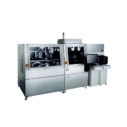

LFB-2301
產品說明
Flip Chip Bonder for TCB process
- Chip-to-Wafer Flip chip bonder for NCF-TCB process
- Capable of high-speed, high-precision flip chip bonding by adopting probe camera technology and linear motor
- High precision control of both bond head force and Z position
- Shinkawa’s NRS technology reduced vibration that obstructs fine pitch bonding
- High throughput achieved by short heating and cooling with pulse heater
- Automatic product-type changeover function with capability to bond up to 4 different product-type chips enables handling of 2.5D and 3D stack packaging
- Capable of handling each plunge-up method and thin die pickup
- Capable of handling 12-inch chip wafer and base wafer
- Molten solder detection function and high-precision Z control reduce damage on devices (under low force mode)
- Process monitoring and management function securing stable quality and process portability
Specification
| ITEM | DETAILS | |
| Product Name | Flip Chip Bonder | |
| Model | LFB-2301 | |
| Bonding Method | Pulse heat thermocompression | |
| Bonding Accuracy | ±2μm (3σ) by Shinkawa’s standard condition | |
| Machine Cycle Time | 2.2s/chip (excludes process time) by Shinkawa’s standard condition | |
| Bonding Force | 1 - 300N ※Capable of selecting bond force control method at bonding process However, it is not capable of switching over between low force control and high force control in the identical bond profile
|
|
| Bonding Tool Setting Temperature | RT - 400℃ (in 1℃ increments pulse heat) | |
| Bonding Stage Setting Temperature | RT - 150℃ (in 1℃ increments pulse heat) | |
| Chip Size | □2 - 20mm t=0.05-0.7mm | |
| Chip Wafer Size | φ200mm, φ300mm | |
| Base Wafer Size | φ200mm, φ300mm | |
| Process | L : 120 – 300 mm, W : 40 – 200 mm (Max 450mm option), t : 0.2 – 2.5 mm | |
| Option Available | Face down/Face up (Option/Other conditions available on request) | |
| Utilities | NCF-TCB | Option available:NCP-TCB, Flux-TCB |
| Communication Interface SECS Ⅰ/ SECS Ⅱ, HSMS, GEM | ||
| Electricity | 5.0kW Maximum | |
| Power Consumption | 5.0kW Maximum | |
| CDA | 570kPa (5.7kgf/cm2) 250L/min Connection:φ10 Tube 1spot | |
| Vacuum | Below -74kPa (-550mmHg) (gage) Connection:φ10 Tube 3spots | |
| Physical Dimensions and Mass | Approx. 3,292W×1,521D×1,701H mm Approx 3,000kg (excludes monitor display, signal tower and load port) | |
※ Specifications subject to change without prior notice.
