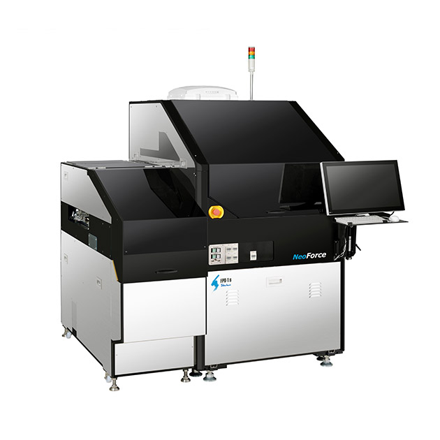

FPB-1ws NeoForce
產品說明
Package Bonder for Multiple Processes
- Chip-to-Wafer package bonder for TCB process
- Capable of switching to Chip-to-Substrate bonding for TCB process within short period of time
- Capable of handling face down process (face up process as an option)
- Capable of handling several kinds of processes such as TCB (NCP/NCF/TC-CUF), C2 and C4, and FO-WLP
- High-accuracy bonding achieved by adopting the unique Non-vibration System (NVS) technology
- Capable of handling high force up to 350N with Force Free Gantry (FFG)
- High throughput achieved by short heating and cooling time with high-speed pulse heater
- Flexibility to handle various plunge-up systems, enabling thin die handling
- Automatic product-type changeover function with capability to bond up to 4 different product-type chips, enabling 2.5D and 3D stack packaging
- High-productivity and space-saving footprint by adopting multiple heads
Specification
| ITEM | DETAILS | |
| Product Name | Package Bonder | |
| Model | FPB-1ws NeoForce | |
| Bond Process Handling Capability | TCB processes (NCP/NCF/TC-CUF), C2 and C4 processes, FO-WLP process | |
| Bonding Accuracy | ±2.5 μm(3σ) Based on bonding conditions at Shinkawa | |
| Machine UPH | UPH6,000 (C4 mode / process time not included) Based on bonding conditions at Shinkawa | |
| Bonding Force | 0.3–350N ※Capable of selecting bond force control method at bonding process However, it is not capable of switching over between low force control and high force control in the identical bond profile. ・Low force control mode:0.3–20N ・High force control mode:10–350N |
|
| Bonding Tool Setting Temperature | RT–400℃ (1℃/Step, Pulse heat) | |
| Bonding Stage Setting Temperature | RT–200℃ (1℃/Step) | |
| Chip Size | □1–22 mm t=0.02–0.7 mm | |
| Chip Wafer Size | φ200 mm, φ300 mm | |
| Base Wafer Size | φ300 mm (φ200 mm Option) /Substrate | |
| Bonding Direction | Face down / Face up (Option/Other conditions available on request) | |
| Options Available | Communication interface SECSⅡ, HSMS, GEM | |
| Utilities | Input Power Supply | Single Phase AC200V–240V±5% 50/60Hz (Other power supply options available on request) |
| Power Consumption | Maximum 14.0kW | |
| Air | 570kPa (5.7kgf/cm2) 300L/min Connection:φ10 Tube x 3 spots | |
| Vacuum | Below -75kPa (-550mmHg) (gage) Connection:φ10 Tube x 3 spots | |
| Physical Dimensions and Mass | Approx. 2,520W × 1,620D × 1,750H mm Approx. 3,100kg (excludes monitor display and signal tower) |
|
※Configuration and specifications of this machine may be subject to partial modification without prior notice.
